WHY HPC WILL REQUIRE
SEMICONDUCTORS BEYOND SILICON?
Transforming semiconductor design with advanced technologies beyond silicon.
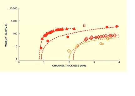
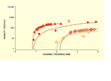
1. MOBILITY DEGRADATION
Mobility degradation is a critical issue for future transistor nodes because it directly impacts performance and power efficiency. This degradation poses a barrier to the continuation of Moore’s Law. However, 2D and 1D materials offer a promising alternative due to their ability to maintain high mobility at ultra-scaled dimensions, potentially overcoming the limitations of Silicon.
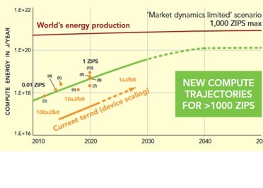
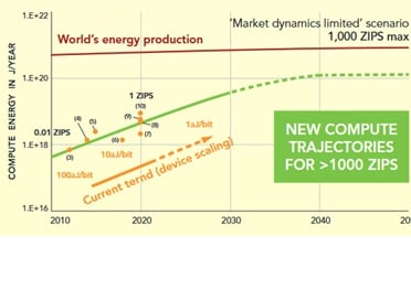
2. POWER CONSUMPTION
As AI and HPC tasks grow in complexity and size, the energy required to support them increases exponentially. This makes it challenging to scale up operations sustainably. The energy consumption of data centers is projected to account for up to 21% of the world’s electricity supply by 2030. High energy consumption translates also into higher operational costs for data centers. This includes not only the cost of electricity but also the expenses related to cooling systems needed to prevent overheating of the hardware.
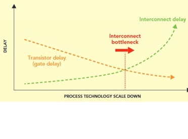
3. INTERCONNECT BOTTLENECK
As the size of transistors continues to shrink, the performance improvements from scaling down the ICs are increasingly limited by the interconnects, which are the pathways that connect different parts of the chip. The interconnect bottleneck is a major challenge in high-performance computing, affecting the latency between memory and digital building blocks. Addressing this bottleneck is crucial for continuing to improve the performance and scalability of computing systems.
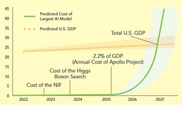
4. COST
High energy consumption translates also into higher operational costs for data centers. This includes not only the cost of electricity but also the expenses related to cooling systems needed to prevent overheating of the hardware. Assuming that compute per dollar is likely to double roughly every four years, or even every two years, the compute trendline still quickly becomes unsustainable before the end of this decade.

ADVANTAGES ENABLED BY IDEADED’S
CNTFET TECHNOLOGY
Transforming semiconductor design with advanced technologies beyond silicon.

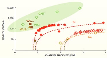
1. HIGH MOBILITY SEMICONDUCTOR EVEN AT EXTREMELY SMALL CHANNELS
CNT’s one-dimensional structure confines electrons to a single path, maintaining high mobility. Additionally, the high aspect ratio of CNTs helps preserve consistent electrical properties over varying channel lengths, making them advantageous for use in transistors as device dimensions shrink.
2. IMPROVEMENT IN TRANSISTOR DENSITY AND INTERCONNECT BOTTLENECK
CNTs can be processed at lower temperatures (less than 400ºC) compared to traditional silicon-based technologies. This allows for the integration of multiple layers of circuits without damaging the underlying layers, enabling the creation of true 3D integrated circuits. By stacking multiple layers of CNT-based circuits, it is possible to create dense 3D architectures. The monolithic 3D integration of logic and memory devices can be realized which can greatly improve the comprehensive performance of the chip and lead to a thousand-fold performance increase for special data structures, especially in AI applications, where IDEADED technology is disruptive.
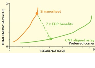
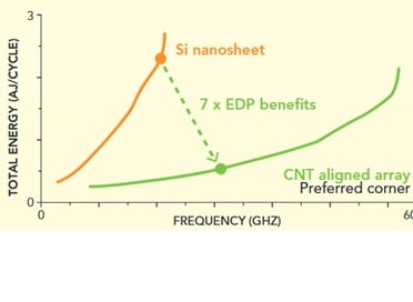
3. LOWER POWER CONSUMPTION
Transistors based on carbon nanotubes (CNTs) offer lower power consumption due to their high electron mobility, which allows for efficient electron movement, and reduced leakage currents that minimize power loss. They can operate at lower voltages (<0.5V), further decreasing power usage, and their efficient switching capabilities reduce the energy required for each operation. Additionally, CNTs’ excellent thermal conductivity aids in effective heat dissipation, reducing the need for extra cooling and contributing to overall energy efficiency.
Innovation
Leading the way in semiconductor technology advancements.
Contact
© 2025. All rights reserved.


IDEADED HELLO
IDEADED TALENT